


Read the Full Series
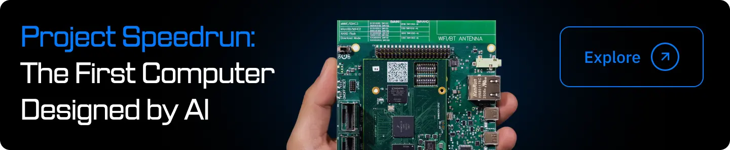
This article is one part of a walkthrough detailing how we recreated an NXP i.MX 8M Mini–based computer using Quilter’s physics-driven layout automation.
What Makes a PCB Tool Truly “Best-in-Class” Today?
“Best-in-class” used to mean deep features and a stable autorouter. Today, it means velocity with confidence—especially for consumer electronics where teams iterate fast and ship often. Here’s the modern checklist.
1) Iteration speed is everything
Consumer devices live on tight, immovable dates (retail resets, seasonal launches, carrier windows). Your tool should turn “try three stackups and two board outlines” from a two-week task into an afternoon. Abundant iteration (not cautious, single-path execution) wins in CE.
2) Native compatibility with your workflow
Mechanical, electrical, and manufacturing must stay in lock-step. A best-in-class tool should ingest native CAD projects (Altium, Cadence, KiCad, etc.), preserve constraints, and hand you files back in the same format for DRC, polish, and fab. No brittle conversions. No “new tool, new process” tax.
3) High-density, high-speed competence
Phones, wearables, audio, AR/VR, smart home—most CE boards are multi-layer, HDI, impedance-controlled, and often EMI-sensitive. Your tool must treat differential pairs, return paths, bypassing, controlled impedance, and keepouts as first-class citizens, not as afterthought rules.
4) Automation that’s more than an autorouter
Classic autorouting reduces keystrokes; modern automation reduces decisions. Expect AI-assisted placement that respects floorplans, thermal/EMC constraints, and manufacturing realities. Expect automatic panelization suggestions and variant management baked in.
5) Team collaboration and traceability
Distributed teams need design review that is transparent: what was auto-placed vs. human-placed, which constraints drove a decision, and what’s left to verify. Tight integration with Git/PLM/issue trackers matters less than the ability to explain layout choices fast.
Bottom line: A top-tier tool accelerates options (more candidates in less time) while raising confidence (physics-aware checks earlier and continuously). That’s the bar.
Here’s How Traditional PCB Software Stacks Up
Legacy PCB tools are powerful. They’ll still be the place you run final DRC, polish, run fab outputs, and archive. But their automation assumptions were built for yesterday’s pace.
Strengths (credit where it’s due)
- Altium Designer: Unified environment, rich 3D ECAD-MCAD, good rules engine, broad CE adoption.
- Autodesk Eagle (now within Fusion): Accessible and integrated with Fusion for tight mechanical fit.
- KiCad: Open-source, rapidly improving, strong 3D and community libraries; great for cost-sensitive teams.
- OrCAD/Allegro: Enterprise-grade constraint management and signal integrity for complex, high-speed designs.
- DipTrace: Intuitive UX, quick ramp for smaller EC teams and prototyping.
Where these tools hit the ceiling for CE velocity
- Manual effort scales poorly. “Smart” autorouting still expects you to place with extreme care and encode dozens of rules perfectly. That’s slow at CE densities.
- Iteration friction. Generating three good candidates (new stackup, new outline, new connector orientation) is days of careful re-work—not hours. You get one shot, not ten.
- DFM is late-stage. Panelization, spacing for high-volume assembly, stencil aperture tweaks, fiducials, test access, and design variants often get validated after layout—not during.
Automation is local, not systemic. Macros/rules reduce clicks, but they don’t reason about physics trade-offs across the whole board.
Traditional tools remain essential. But for CE teams pushing density and deadlines, pairing them with AI turns your CAD from “where work happens” into “where finalization happens.”
How Does AI Change the Game for PCB Layout?
AI at its best isn’t a black-box autorouter—it’s a physics-driven collaborator that understands your constraints, your manufacturing reality, and your deadline.
Physics-aware placement and routing
AI can identify bypass networks, impedance-controlled nets, diff pairs, return paths, and EMI-sensitive loops. Instead of just honoring trace width rules, it reasons about field effects and current flow, placing components and routes to minimize coupling and noise from the start.
Automated, continuous DFM
Rather than waiting for a manufacturing DFM report, AI evaluates clearances, component spacing, AOI reach, pick-and-place stability, fiducials, test access, and stencil risk while it places and routes. It can propose panelization patterns that balance utilization with assembly line throughput.
Parallel candidate generation
Give the AI your constraints and let it spin dozens of viable layouts: different stackups, alternative connector orientations, variant BOMs, or enclosure-driven outlines. You review the trade-offs (EMI margin vs. SSD thermals vs. assembly time) instead of hand-crafting each candidate.
Fits your stack, not fights it
Best-in-class AI plugs into your current toolchain: submit native Altium/Cadence/KiCad, get native files back. You still run final DRC, tweak silks, and export Gerbers where you’re comfortable.
Net-net: AI shifts effort from manual keystrokes to strategic choices. You spend time evaluating options, not wrangling them into existence.
What Results Can You Expect From AI-Driven PCB Design?
Direct answer :
AI-driven PCB tools typically cut layout time from weeks to hours, reduce respins via built-in manufacturability and physics checks, lower assembly cost and failure rates through smarter spacing/panelization, and accelerate time-to-market by enabling more design iterations in less time.
Expanding on that:
- Weeks → hours for first-pass layout. With AI handling placement/routing under your rules, first-pass layouts land quickly—so you can test earlier, learn sooner, and iterate more.
- Fewer board turns. Early, continuous DFM and physics checks catch issues that normally surface during EVT/DVT. Expect fewer re-routes for EMI, thermals, or assembly surprises.
- Lower COGS and field returns. Smarter panelization and assembly-friendly design reduce feeder swaps, rework, and yield loss. Better return paths and decoupling reduce field failures.
- Faster portfolio velocity. With layout unblocked, you can run more SKU variants and A/B mechanical trials in parallel—without adding headcount.
Let’s Talk About Design for Manufacturing: Why It Matters More Than Ever
In consumer electronics, DFM is not paperwork—it’s profit margin and schedule insurance. Historically, DFM lived at the end: you’d send out a candidate, get feedback from the CM, make changes, and try not to slip. That loop doesn’t scale when you’re shipping multiple SKUs across multiple lines.
How AI fixes DFM’s late-stage problem
- Panelization by constraint, not gut. AI can evaluate panel utilization vs. line rate, fiducial strategy, break-tab design, and test-point accessibility, then propose the best panel for your assembly line and lot size.
- Assembly-aware spacing and orientation. It understands nozzle clearance, component fragility, reflow risk, and AOI coverage, and it places with those realities in mind.
- Variant-ready layouts. If you have regional SKUs or feature toggles, AI can preserve test access, reflow consistency, and AOI visibility across variants.
Mini case example: Wearable mainboard (hypothetical but typical)
A smartwatch mainboard (10-layer HDI, tight enclosure) needs to hit two factories with different panel size preferences. The AI generates three candidates:
- Max-utilization panel: best raw PCB cost, tighter AOI margins.
- Balanced panel: slightly lower utilization, improved AOI coverage and feeder change time.
- Throughput-optimized panel: lowest cycle time for Line B; best schedule fit.
The team picks #2 to balance yield and schedule, and ships EVT a week earlier—no surprises at AOI because spacing choices were baked in, not bolted on.
Want a deeper dive? See the DFM Guide inside our documentation to translate panelization theory into line-level decisions. Start at docs.quilter.ai.
Here’s How Quilter’s AI Makes Consumer Electronics PCB Design Faster and Smarter
Quilter was built to work with your current tools while removing the layout bottleneck.
Upload native CAD projects
Submit Altium, Cadence, Siemens, or KiCad projects. Define the board outline, pre-place connectors, lock critical keepouts, and set constraints. Quilter respects your intent from the first run.
→ Explore the Product Overview
Physics-driven layout engine
Quilter detects bypass capacitors, impedance-controlled nets, diff pairs, and other critical considerations upfront. Placement and routing are guided by physics (return paths, coupling risk, EMI/EMC behavior), not just rule width tables.
Generate many candidates—fast
Try multiple stack-ups, form factors, and manufacturers in parallel. In hours, you’ll have a short-list of credible boards to review—each scored against your physical and DFM constraints.
Automated DFM optimization
Quilter bakes in panelization suggestions, assembly-friendly spacing, fiducials, and manufacturability scoring. You see where you’re solid and where you should look closer—before a CM ever sends feedback.
→ Read the Documentation
Transparent design review
Every candidate comes with a clear evaluation: which constraints were satisfied, where margins sit (EMI, impedance, thermals), and what needs human review. That lets leads sign off confidently and juniors learn faster.
Seamless handoff back to CAD
Quilter returns files in the same format you submitted. Run DRC, add silks, generate fab files, and archive in your CAD tools. No new PDM/PLM workflow required.
Support the way CE teams work
- Hardware-rich development: pace your builds with more learning cycles, not fewer.
- Enterprise-grade support: for mission-critical schedules and compliance needs.
- Security: keep your IP in your native toolchain; Quilter integrates without lock-in.
What it looks like end-to-end (60-second tour)
- Upload project + constraints →
- AI proposes placement & routes under physics/DFM constraints →
- You review candidate scores and diffs →
- Select/merge best options →
- Export native CAD for final touches and fab.
→ Watch the short workflow demo on the Product page.
→ Try it hands-on with the Free Version.
Traditional vs. AI-Driven: A One-Glance Summary
- If you need 1–2 careful boards with lots of manual control → traditional CAD alone is fine.
- If you need 5–15 credible options this week, validated against physics and DFM → pair your CAD with AI.
What Results Can You Expect From AI-Driven PCB Design? (Expanded)
- Time: First viable layouts in hours, not weeks.
- Quality: Better EMI/EMC behavior and signal integrity by construction.
- Manufacturability: Higher yields and smoother AOI/P&P from baked-in spacing/panelization.
- Cost: Lower rework and scrap; fewer last-minute expedites.
- Team leverage: Senior designers review more and re-route less; juniors learn from transparent AI decisions.
“We stopped arguing about whether we could hit the date and started comparing which candidate hit DFM and EMI with the most margin.” — Hardware lead, consumer devices (typical sentiment)
Ready to See the Next Generation of PCB Design?
If your team ships consumer hardware on real deadlines, AI isn’t a nice-to-have—it’s how you keep velocity without gambling quality.
- See Quilter in action: fast, physics-aware, DFM-ready. → Product Overview
- Try it free: upload a project and generate candidates today. → Free Version
- Level up DFM: panelization, spacing, AOI/test access guidance. → (https://docs.quilter.ai/)
AI PCB design tools are raising the bar. The teams who adopt them will own the launch window—and the category.
Appendix: Tool-by-Tool Context for CE Teams
- Altium Designer
Best for: mature CE teams needing rich ECAD-MCAD and a powerful rule engine.
Mind the gap: abundant iteration is still manual; DFM is largely post-layout. Pairs well with AI to produce options you finalize in Altium. - Autodesk Eagle (Fusion)
Best for: tight ECAD-MCAD interplay, accessible workflows, and smaller CE projects.
Mind the gap: complex HDI and throughput-optimized panelization benefit from AI pre-work. - KiCad
Best for: cost-sensitive teams and programs that value transparency and community tooling.
Mind the gap: speed at CE density improves drastically when AI handles placement/DFM upfront; finalize in KiCad. - OrCAD/Allegro
Best for: high-speed, enterprise-grade constraint management.
Mind the gap: when schedules are aggressive, AI can hand you multiple compliant candidates to review in Allegro rather than craft from scratch. - DipTrace
Best for: fast ramp-up and smaller boards.
Mind the gap: AI unlocks “bigger than usual” density and faster panelization decisions; finish in DipTrace.
Internal Links for Continuity
Documentation (DFM, workflow, support): https://docs.quilter.ai/


