


Read the Full Series
This article is one part of a walkthrough detailing how we recreated an NXP i.MX 8M Mini–based computer using Quilter’s physics-driven layout automation.
I started my career designing electronics for spaceflight at SpaceX, focusing on ionizing radiation effects. On orbit, high-energy particles can wreak havoc on any circuit, so every component and board had to be tested in radiation facilities here on Earth.
The problem was timing. Testing a finished avionics box was often “too late.” If it failed, you risked delaying a launch. The smarter approach was to screen components earlier—before they even entered the design library. With thousands of parts in a spacecraft, that meant designing dozens of specialized test boards every year.

Source: Radiation Test Board by ESA
And this isn’t unique to aerospace. Automotive, medical, and semiconductor companies all rely on similar boards for environmental and reliability testing. They’re not especially difficult designs—but they are time-consuming, often taking weeks to design.
This was one of the sparks for starting Quilter. Our goal is to automate PCB design in general. But we realized that if we could start with boards like this, we could significantly accelerate timelines for hardware companies long before Quilter could tackle the hardest boards out there.
To demonstrate that, Ben Jordan built our own 32-sensor array with an FPGA and live visualization. It’s exactly the kind of auxiliary test hardware every R&D team needs, and exactly the kind Quilter can generate in hours instead of days.
Ben Jordan CID+ Staff Electrical Engineer
Ben brings over 20 years of experience in EDA, including 16 years at Altium. As Quilter's staff electrical engineer, he designs real boards that must work.
The Designs that Create the Bottleneck
This board characterizes 32 MEMS accelerometers in parallel—one of the essential but time-consuming fixtures, bring-up platforms, and evaluation harnesses every hardware team must build.
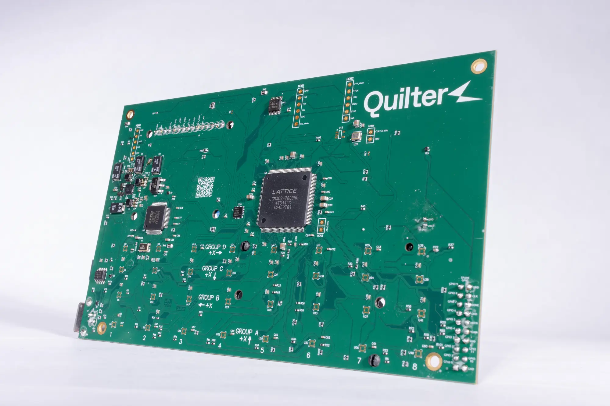
- 32x MC3479 accelerometers with digital compass on I²C
- Lattice MachXO2 FPGA running a soft RISC-V core in fabric
- Linear Technology power management IC with three switching regulators
- USB 2.0 (480 Mbps) with integrated JTAG
- TFT display for real-time visualization via SPI
- Nearly 100 bypass capacitors
Auxiliary boards block programs everywhere:
- Fixtures to test sensors before multi-million-dollar production commits
- Bring-up boards to validate new silicon
- Characterization platforms to build reliability data
- Interconnect boards to stitch subsystems together
Auxiliary boards block every program: fixtures to test sensors before multi-million-dollar commits, bring-up boards for new silicon, characterization platforms to validate reliability, and interconnect boards to link subsystems.
A “two-day” layout task cascades into weeks of idle teams and delayed launches.
Designing with Quilter
Ben spent about 30 minutes preparing the design for Quilter.
.webp)
- USB connector and power jack (edge access required)
- TFT display header (cable length constraint)
- LED array and switches (front panel alignment)
- Mounting holes (enclosure compatibility)
- 32-accelerometer grid (4×8 array with varied orientations for comparison)
- Lattice iCE40 FPGA and all supporting circuitry
- Linear Tech power management IC with three regulators
- Nearly 100 bypass capacitors
- All discrete components and passives
- Bulk storage capacitors
- Power distribution architecture
He manually placed less than 20% of the components. Everything else—FPGA support circuitry, regulators, nearly 100 bypass caps—was left unplaced. Quilter recognized the structure of the array, preserved the test intent, and optimized the rest.
Two Hours Later
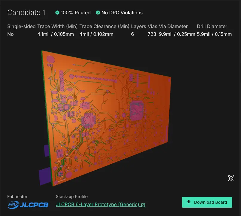
Quilter produced multiple complete candidates. Ben chose a six-layer version with a single lamination cycle. It wasn’t the cheapest or the prettiest, but it was the most pragmatic:
- Single lamination = faster turnaround, lower cost
- Unbroken planes between signal layers = inherent signal integrity
- Broad manufacturer compatibility
- All physics constraints validated
“A human artist might complain it doesn’t look hand-routed. I don’t care about that. I care that it works and lets me move on.” — Ben Jordan
Post-processing was minimal—denser via stitching, silkscreen cleanup—less than an hour of work.
From Gerbers to Working Hardware
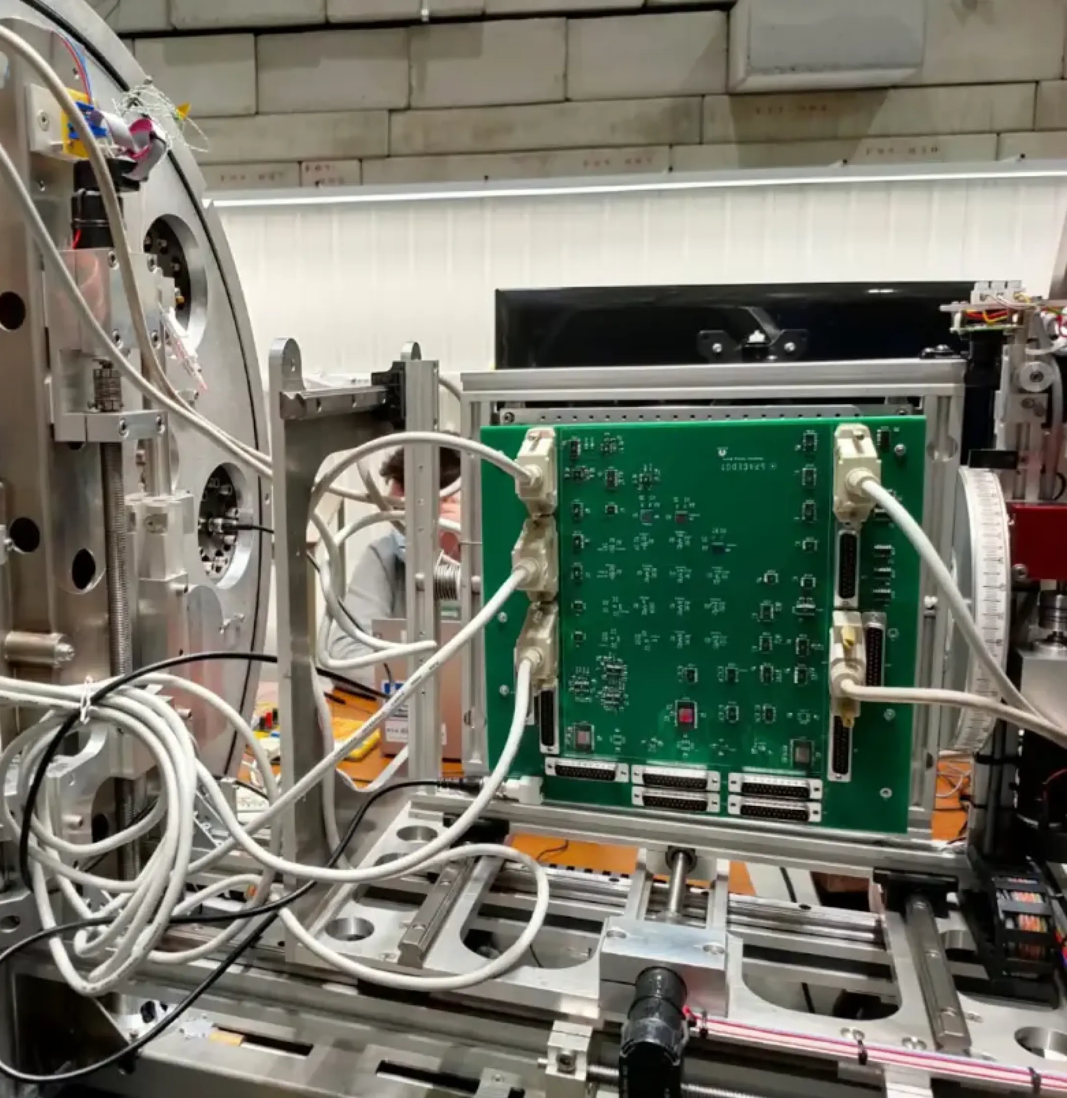
Five boards were fabricated and assembled offshore: six layers, capped vias. All but the debug-sacrificed unit powered up and ran continuously, producing clean characterization data. We assembled offshore to keep costs low, but any local quick-turn fab would have had no problem turning this board around in days.
.webp)
- 5 boards fabricated and assembled offshore
- 6 layers, plugged and capped vias
- Total cost: under $600
- Zero manufacturing holds or clarifications
With the display connected and firmware loaded, the complete system comes to life. The FPGA initializes the TFT controller over SPI, verifies register reads, and drives live updates to the screen. The logic analyzer confirms correct timing and command sequencing—proof that the hardware, firmware, and routing all behave exactly as designed. The board powers on, measures, communicates, and visualizes sensor data in real time.
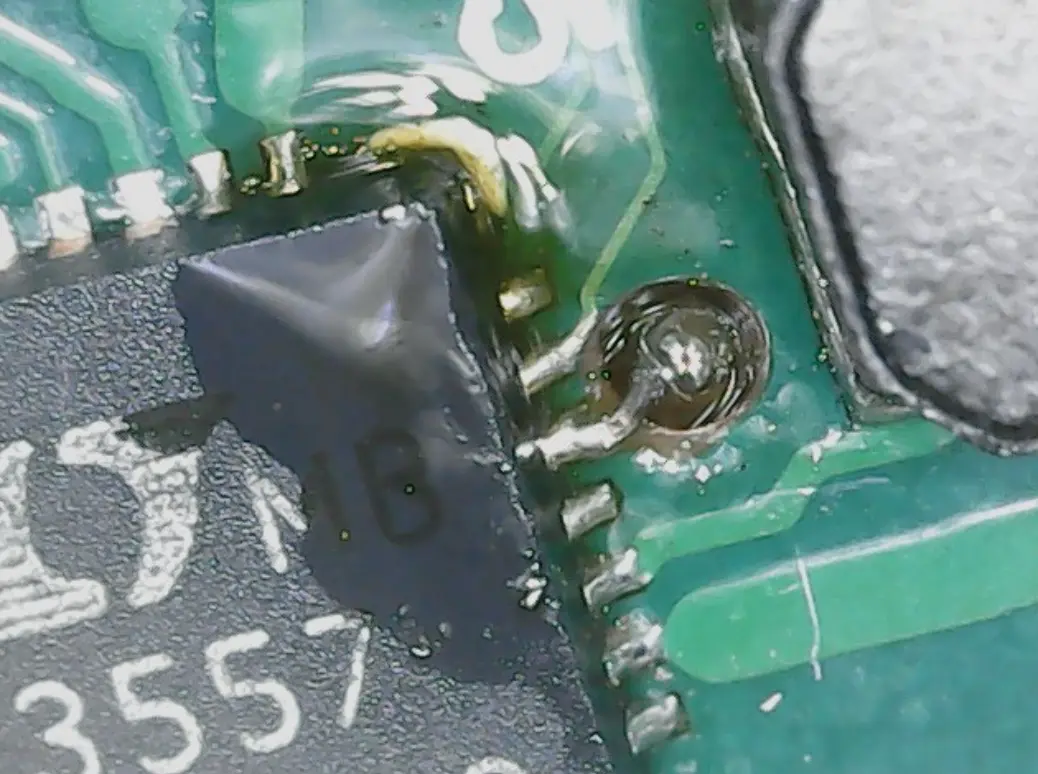
Side Quest
One schematic error slipped through: a regulator pin left floating instead of tied to ground. Quilter implemented the schematic faithfully.
- Dremel with micro drill bit through PCB
- Microscope-assisted soldering
- Hair-thin wire from pin 19 to ground plane
- One board sacrificed to diagnosis
- Four boards successfully modified


Learning
This board was done in Jan ‘25. We took a lot of lessons from it, and have made Quilter better.
.webp)
The biggest lesson for us was to put a lot more attention on bypass cap placement — especially in dense designs. We’ve drastically improved our representation of the place-able space, and improved the core optimization algorithms, leading to excellent bypass cap proximity even in very space-constrainted designs. For example, see below an RP2040 design where bypass cap associations are shown in purple.
%201.webp)
Another key effort was to improve our power distribution. At the time that we built this sensor array, we were just routing power with thick traces. But the better thing to do is to use much larger power polygons to minimize the inductance. So, Quilter now has the ability to create polygons for power nets (in addition to creating a dedicated power plane):
.webp)
The Time Multiplier Effect
A pro designer like Ben who knows Altium inside and out could have designed this board in just a couple of days. But speaking from my own experience at SpaceX - it is seldom the case that a pro of that calibre has time for a project like this. In reality, the PCB layout team is too busy with flight-critical designs, which means that this burden rests on the schematic designer or test engineer, for whom layout is not typically the focus. So, boards like this end up taking a week, and not just a couple of days.
Instead of spending his time on the layout, Ben was able to focus on everything else that needed to be done to get this board up and running:
- HDL for FPGA: Custom logic interfacing 32 I²C buses simultaneously
- RISC-V implementation: Soft processor running in FPGA fabric
- Bare-metal drivers: Direct hardware control for maximum performance
- Display controller: 40 MHz SPI interface with real-time visualization
- Mechanical design: 3D-printable enclosure in Fusion 360
- Protection system: Robust brackets preventing TFT damage
"I was able to get on with firmware development... that honestly took a lot more of my time."
That's the revelation. The hard problems aren't routing traces—they're making systems work. Reading vendor documentation. Understanding FPGA timing. Creating robust drivers. The work that actually ships products.
Take Action Today
Learn More about and get started with Quilter today: https://quilter.ai/learn-more