


Read the Full Series
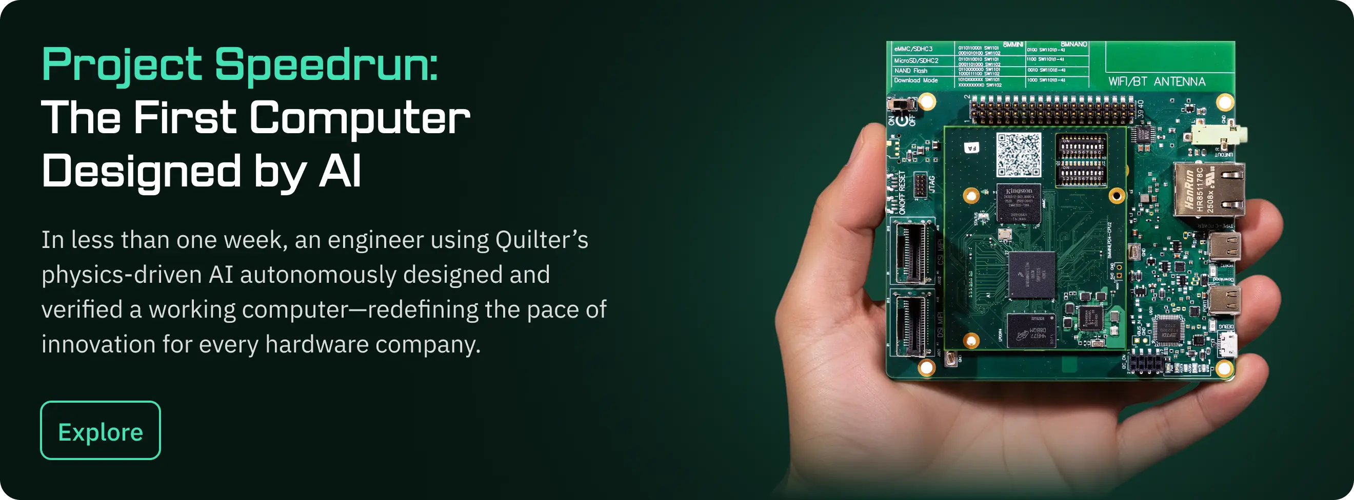
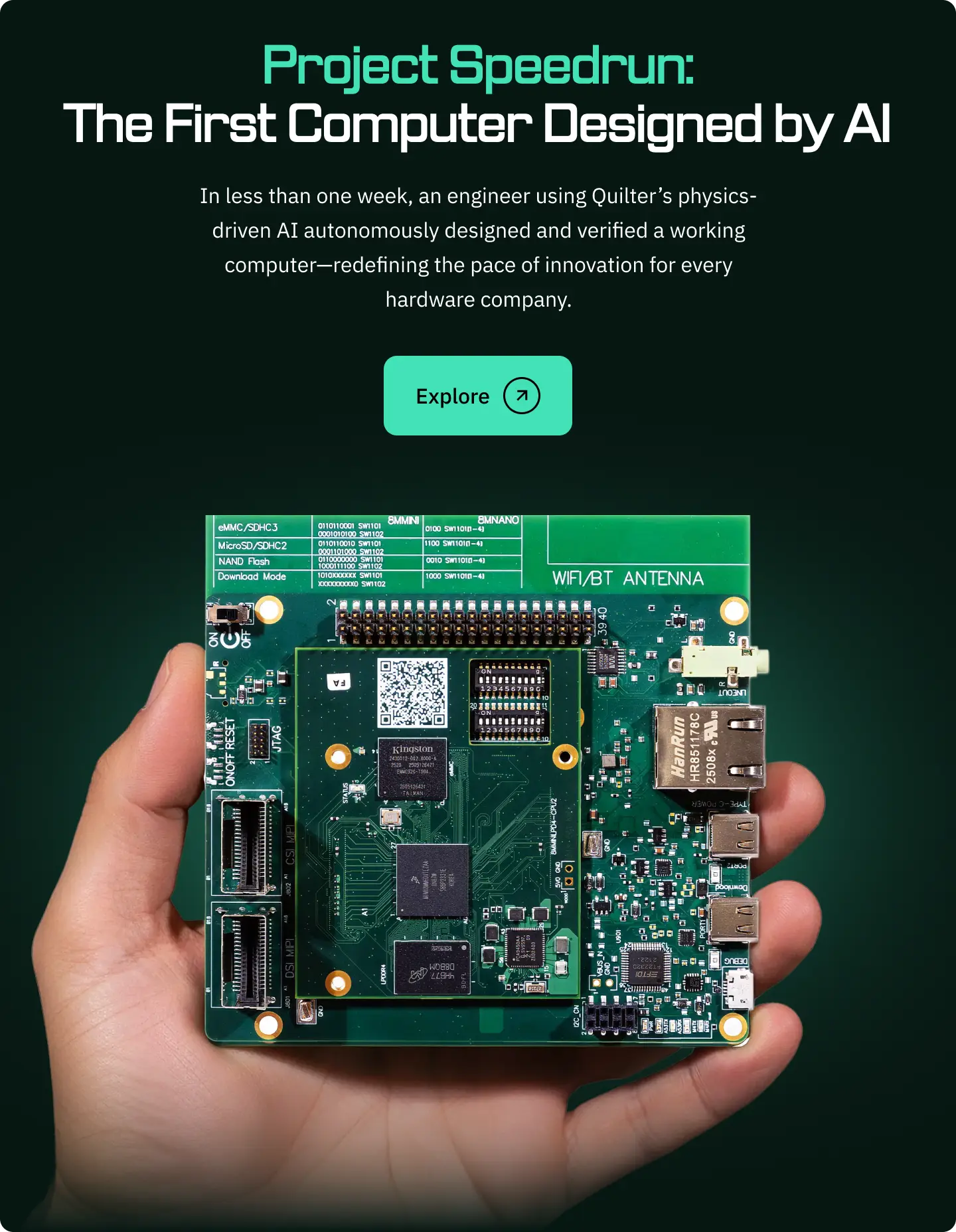
This article is one part of a walkthrough detailing how we recreated an NXP i.MX 8M Mini–based computer using Quilter’s physics-driven layout automation.
Choosing PCB layout software isn’t just a tooling decision—it’s a schedule decision. In 2025, the gap between teams who ship and teams who slip usually comes down to one thing: how fast you can move from schematic to a manufacturable board with confidence. This review breaks down what “efficiency” really means in PCB layout, compares the top tools engineers rely on today, and shows how Quilter’s physics-driven AI changes the equation for high-velocity hardware teams.
Let’s define what makes PCB layout software truly efficient
“Efficient” is not the same as “fast autorouter.” If you complete a route quickly but spend days untangling vias, fixing differential pair mismatches, and chasing EMI or return-path problems, you didn’t save time—you postponed it.
When we talk about efficient PCB layout software, we’re talking about the total design cycle:
- Time-to-first manufacturable candidate: From a ready schematic and constraints to a layout candidate that passes review and can head toward fab.
- Manual cleanup load: The number of post-route adjustments (length tuning, via fences, stitching, keepout fixes) needed to make the board actually shippable.
- Iteration speed: How quickly you can explore alternate placements, stack-ups, and manufacturers—because better options often appear when trying costs almost nothing.
- Physics-aware validation: Early detection of issues that typically surface in late DRC, lab bring-up, or—worst case—after a re-spin.
- Fit with your workflow: Native file compatibility, handoff back to your CAD, and low onboarding friction so your team can adopt improvements without process churn.
In short: efficiency is about reducing total calendar time and risk, not just making traces appear faster.
What are the top PCB layout tools engineers use today?
There are great tools in the market, and most teams will continue to use at least one of them for years. Here’s the quick landscape.
Altium Designer
The enterprise workhorse. Unified environment, powerful rules/routing, length tuning, xSignals, strong 3D/MCAD collaboration. Ideal for complex, multi-layer boards where process control and design governance matter.
KiCad
Open-source and increasingly capable. Modern interactive routing, length tuning, solid library ecosystem, and active community. Excellent for cost-sensitive teams, research labs, and professional projects that don’t need proprietary vendor lock-in.
Autodesk Eagle
Lean, approachable, and integrated with Fusion 360 for MCAD. Well-liked for rapid prototyping and small to mid-size projects. (Many legacy projects still live here.)
DipTrace & EasyEDA
Approachable, accessible options. EasyEDA’s browser-first model and fab integrations make it popular for quick turns; DipTrace is appreciated for its clean UI and straightforward routing for small teams.
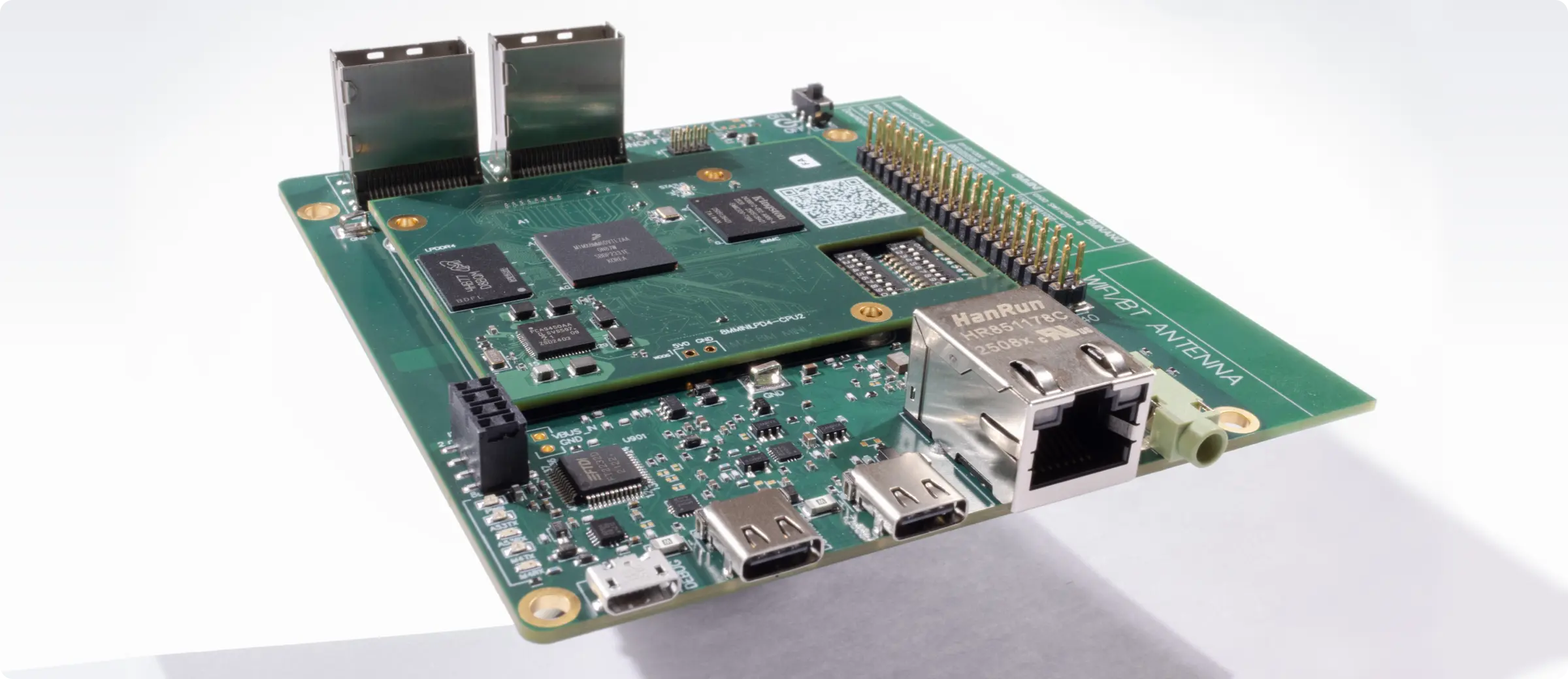
Quilter
A physics-driven AI PCB layout tool that sits alongside your current CAD. You upload native Altium/Cadence/Siemens/KiCad projects, define constraints, and Quilter generates multiple layout candidates in parallel, runs physics-aware checks, and returns native files for final polish and fabrication.
At a glance
- Traditional tools are excellent “do-everything” environments with strong manual and semi-automated routing.
- Quilter is an automation engine focused on efficiency: generating and validating manufacturable layouts quickly, giving you time back and reducing iteration risk.
Here’s how Quilter approaches efficiency differently
Think of traditional PCB layout like crafting a single, painstaking route. You can be incredibly skilled and fast, but you’re still making one candidate at a time.
Quilter flips that model:
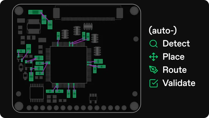
- Physics-first understanding of your design intent
Quilter ingests your native CAD project and automatically identifies impedance-controlled nets, differential pairs, bypass capacitors, keepouts, stitching strategies, and other constraints you specify. You approve what Quilter will and won’t account for—up front. - Reinforcement learning for multi-candidate generation
Instead of producing one route, Quilter trains against your constraints and generates multiple layout candidates in parallel—each one a different valid approach to placement, routing topology, and via strategy. - Automated physics checks
Candidates are evaluated against the physical realities that make or break first-pass success: return paths, length/phase budgets, diff-pair quality, stitching via density, EMI-sensitive regions, power distribution sanity, and manufacturability rules. - Native handoff back to your tools
Quilter returns the same file type you uploaded (Altium, Cadence, Siemens, or KiCad). You run your usual DRC, finalize silkscreen/labels, and generate fab files—no rip-and-replace.
In plain language: Quilter gives you more good options, faster, and validates them against physics before you ever hit the lab. That’s where the calendar time disappears.
How does Quilter’s efficiency compare to other PCB tools?
We ran a benchmark across three representative board classes (2-layer MCU, 4-layer mixed-signal with RF keepouts, and 8-layer DDR/PCIe + 2.4 GHz RF). Designers with professional time in each tool followed written procedures and consistent constraints. Quilter generated multiple candidates; the best physics-validated result was exported back to native CAD for final checks.
Quilter delivered validated layouts up to ~7× faster than traditional flows, with ~70–80% fewer manual cleanup steps and ~10–17% fewer vias on average across the tests. That translates into tighter schedules and fewer re-spins.
Snapshot comparison (representative averages)
Notes: Values are representative ranges/patterns from our tests and user deployments. Traditional tools can and do ship complex boards; the difference is time recovered and manual effort avoided.
What results can you expect when switching to an AI-powered workflow?
Teams usually see three improvements—fast.
- Shorter critical paths
When layout stops eating the schedule, your bottlenecks move where they should be: silicon lead times, firmware, and mechanical integration. Across mixed-signal boards, we’ve seen teams reclaim days to weeks. - More design exploration, same headcount
Because Quilter makes candidates “cheap,” teams try more placements, more stack-ups, and alternate manufacturers. More exploration → better designs → fewer costly surprises. - Higher first-pass confidence
Physics-aware checks surface issues early, reducing re-spins. Engineers spend more time on system-level trade-offs and less on repetitive routing cleanup.
User quote (engineering manager, consumer electronics):
“We cut four weeks off bring-up on an 8-layer board and hit a holiday build we thought we’d miss. Our designers are still using Altium for final polish, but Quilter does the heavy lifting. It’s a force multiplier.”
User quote (validation hardware lead, semiconductor):
“The win isn’t just speed. It’s the parallelism. I get multiple viable layouts to choose from, with the physics checks already done. That changes how we plan the entire program.”
Getting started: What to know before you try Quilter
You don’t have to change your stack. Quilter works with the tools you already use:
- Upload: Altium, Cadence, Siemens, or KiCad projects.
- Set constraints: Board outline, pre-placed connectors, keepouts, impedance targets, diff-pair budgets.
- Generate: Quilter creates multiple physics-validated candidates in hours, not weeks.
- Handoff: Receive native files back for DRC, silkscreen, and fab in your CAD.
Practical tips for a fast first win
- Start with a live project, not a toy example. Choose a board where layout is on the critical path.
- Provide clear, auditable constraints (impedance, length budgets, keepouts, stitching density).
- Use the candidate comparison report to pick the best layout—don’t overthink it. Merge small preferences in your CAD afterward.
- Keep your existing release process (DRC, ECNs, CAM)—Quilter fits in, it doesn’t replace.
Ready to see how much faster your team can move? Try Quilter for free or schedule a demo with our engineers.
Appendix: Why “efficient” now means physics-driven—and parallel
The historical pattern is familiar: smarter interactive routers, better rules, tighter DRCs. All valuable. But they still revolve around one candidate at a time and lean heavily on manual expertise to avoid late-stage issues.
Physics-driven + parallel is different:
- It front-loads validation so you avoid “gotchas” that appear only after days of cleanup or in the lab.
- It multiplies options, letting you compare topologies in hours—not argue about them for weeks.
- It returns native files, so you keep your institutional knowledge and release flow untouched.
That’s why teams describe Quilter not as “another CAD tool,” but as an efficiency engine that sits beside CAD and collapses time everywhere layout used to slow them down.
Frequently asked questions
What is the most efficient PCB layout software in 2025?
For teams optimizing total cycle time, Quilter stands out by generating multiple physics-validated layout candidates in hours and handing back native CAD files. Traditional tools like Altium and KiCad remain excellent for finalization and ecosystem depth; the efficiency gain comes from Quilter’s parallel, physics-aware automation.
Do I need to abandon my current toolchain?
No. Quilter ingests and returns your native files (Altium/Cadence/Siemens/KiCad). Keep your DRC, documentation, and fab workflows unchanged.
Does Quilter help on simple boards too?
Yes, but the biggest wins appear on mixed-signal and multi-layer high-speed/RF designs where manual cleanup and late-stage surprises typically burn calendar time.
How do you measure “efficiency”?
Time to first manufacturable candidate, manual adjustments required post-route, via count/topology quality, physics-aware checks passed, and iteration speed across multiple candidates.