


Read the Full Series
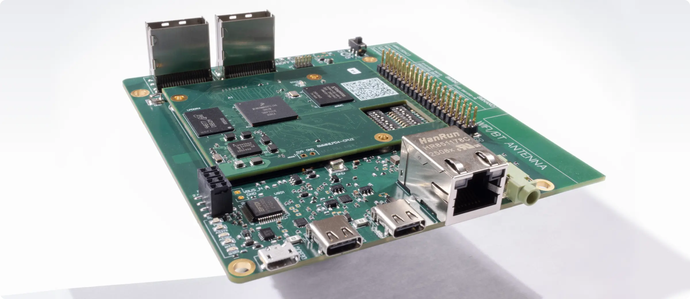
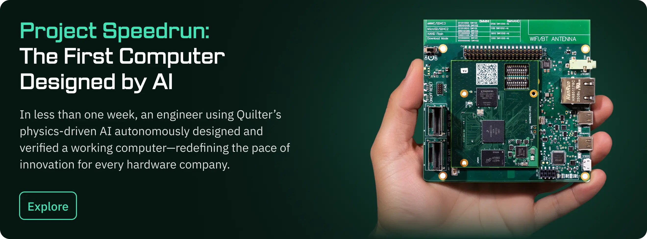
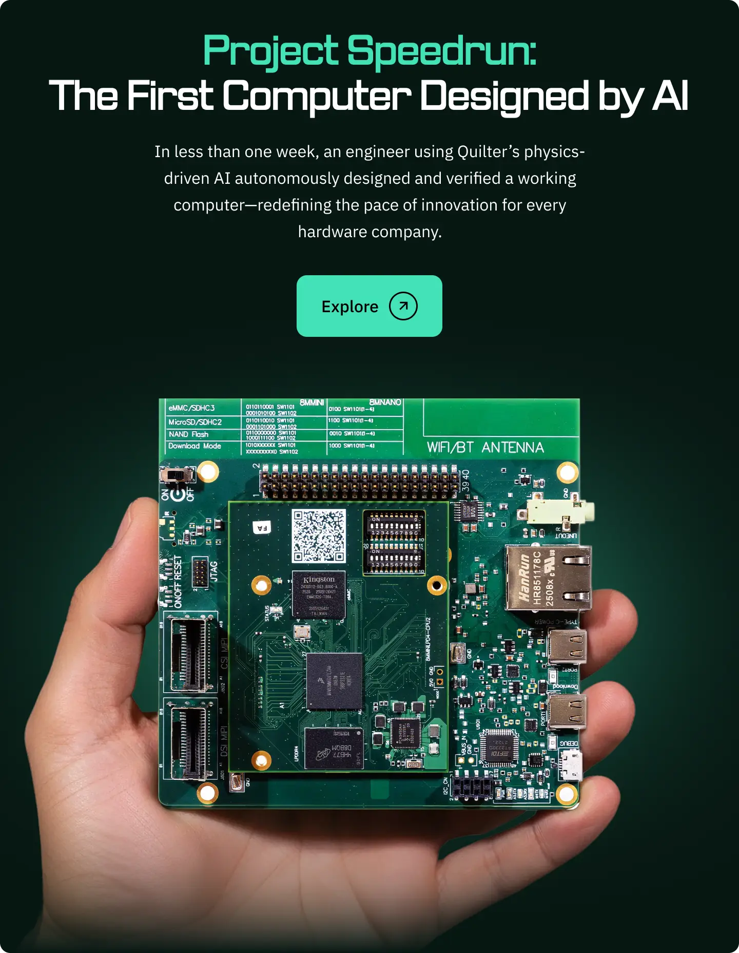
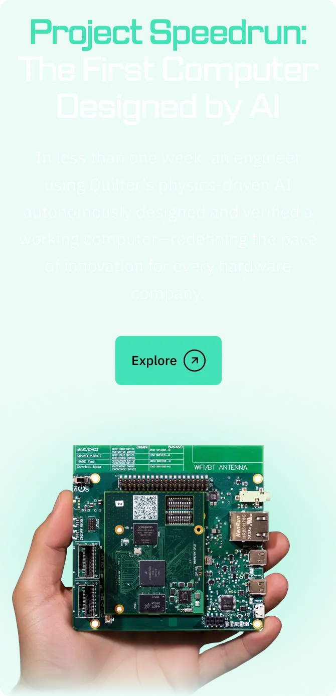
This article is one part of a walkthrough detailing how we recreated an NXP i.MX 8M Mini–based computer using Quilter’s physics-driven layout automation.
Introduction: Why Efficiency Matters More Than Ever in PCB Layout
In 2025, the difference between shipping hardware on time and missing your window often comes down to one thing: how quickly you can go from schematic to a finished, manufacturable board. We set out to answer a simple question: which PCB layout software actually delivers the fastest, most efficient results when you’re under real engineering constraints?
Traditional layout tools are powerful—no debate there. But they’re also shackled by the same bottleneck we’ve all wrestled with for years: manual iteration. Every change to the stack-up, every floorplan revision, every EMI tweak ricochets through hours (or days) of rework.
AI-driven, physics-aware layout flips that script. Instead of grinding through one layout at a time, you generate multiple candidates in parallel, validate them against real physical constraints, and ship the one that meets spec earliest.
This post is the data: a head-to-head benchmark of Quilter, Altium Designer, and KiCad across three representative boards. Real layouts, reproducible constraints, and a transparent methodology you could replicate tomorrow.
What Does “Efficiency” Really Mean for PCB Layout in 2025?
“Efficiency” isn’t just raw autorouter speed. If you win the race and still spend hours un-snarling vias and fixing impedance issues, you didn’t win much. We defined efficiency with three practical, engineering-relevant metrics:
- Total routing time (minutes)
From a validated schematic and ruleset to a completed layout candidate ready for DRC, review, and fab preparation. This reflects real time you can recover in a development cycle. - Manual adjustments (count)
Number of human interventions required post-routing to pass review. Think: via fences that need to move, length mismatches that must be tuned, guard rings added, diff-pair meanders fixed. Fewer interventions = less calendar slip. - Via count (absolute)
Vias aren’t inherently bad, but excess vias can indicate longer current return paths, unnecessary layer changes, and potential SI/PI risks. We used via count as a pragmatic proxy for topological optimization.
These metrics matter to engineers (less thrash) and managers (tighter schedules, lower risk) alike. They also translate to cash: fewer hours, fewer spins, faster bring-up.
How Did We Benchmark Quilter Against Altium Designer and KiCad?
If you’ve ever read a “benchmark” that smells like marketing, you know how this goes. We avoided that. Here’s exactly what we did, and how you can replicate it.
Boards tested (three representative classes):
- Simple MCU (2-layer) – 48 MHz MCU, USB FS, regulators, moderate I/O.
- Moderate Mixed-Signal (4-layer) – BLE module, 12-bit ADC front-end, 2 MHz DC/DC, EMI keepouts.
- Complex RF + High-Speed (8-layer) – DDR3L @ 800 MT/s, PCIe Gen2 x1, 2.4 GHz RF, controlled impedance, stitching vias.
Rules & constraints (kept consistent across tools):
- Manufacturer-realistic widths/clearances; controlled-Z on high-speed nets.
- Diff-pair constraints and length matching where applicable (DDR, PCIe, USB).
- Keepouts and placement constraints for RF & power integrity.
- No “secret” tool-specific plugins; out-of-the-box capabilities plus documented features (e.g., interactive routing, XSignals, push-and-shove).
Who performed the tests:
Experienced PCB designers with professional time in all three tools. We rotated operators to minimize tool-familiarity bias and used written test procedures to keep steps consistent.
Workflow differences that matter:
- Altium Designer and KiCad followed a conventional flow: floorplan → placement → interactive/auto routing → tuning → manual fixes per review feedback.
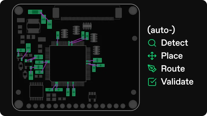
- Quilter followed a physics-driven AI flow: ingest native project → validate constraints/intent (impedance-controlled nets, diff pairs, keepouts) → generate multiple layout candidates in parallel → run automated physics checks → select the best candidate for final review (and optional touch-ups) → export back to the same native CAD format you submitted.
Quilter’s goal isn’t to “win the autorouter race.” It’s to eliminate the bottleneck—by producing multiple physics-aware candidates quickly and letting you choose the one that meets spec with minimal cleanup.
Here’s What the Numbers Show: Efficiency Results Across Three Board Types
To make this review as transparent as possible, we measured three key metrics across three board types. Here’s how Quilter, Altium Designer, and KiCad performed side-by-side:
Optional visuals you can embed in your post or deck (one per board):
- Time to Route — Simple MCU
- Time to Route — Moderate Mixed-Signal
- Time to Route — Complex RF + High-Speed
What the numbers mean (plain English)
- Time recovery is real, not theoretical.
Across the three boards, Quilter reduced routing time by 72–77% vs. Altium Designer and 76–81% vs. KiCad. That’s the difference between a day and a week on mixed-signal, and between a long afternoon and multiple workdays on complex RF/high-speed. - Manual cleanups drop by ~70–80%.
Post-route adjustments fell from 17–129 down to 3–26. That accelerates design review and shortens the path to DRC/fab files. - Via count trends lower with Quilter.
Expect ~10–17% fewer vias across boards. It’s a practical signal that the routing is more topologically efficient (shorter return paths, fewer layer swaps), which often correlates with better SI/PI outcomes and fewer late-stage surprises. - Traditional tools still hold their own in capable hands.
Altium Designer and KiCad produced shippable layouts that passed review. If you live in those tools, you can get the job done. The difference is how fast you get there and how many manual steps it takes.
What Surprised Us Most About the Results?
1) The biggest gains weren’t on the “easy” board—they were on the complex one.
We expected Quilter to dominate the 2-layer MCU board (it did), but the 8-layer DDR+PCIe+RF board is where physics-driven AI really separated itself. Generating multiple candidates in parallel and automatically validating them against impedance, diff-pair, and keepout constraints cut days off the cycle.
2) Manual artistry still matters—for edge-case constraints.
On ultra-specific mechanical constraints or “house style” routing preferences, humans sometimes outperformed default automation. The upside: with Quilter, you start from a compliant, physics-validated baseline and apply those last-mile preferences surgically, not from scratch.
3) Learning curve = short.
Designers who had never used Quilter were productive in a single session. The workflow is intentionally familiar: you upload native Altium/Cadence/Siemens/KiCad projects, set constraints, and get back native files. This mattered more than we imagined—no cultural change, no rip-and-replace.
4) Placement decisions were more consequential than we expected.
When we locked suboptimal initial placement to be “fair” across tools, traditional flows suffered disproportionately. Quilter’s multi-candidate approach effectively explores better placements and topologies in parallel, so poor starting conditions hurt less.
How Can These Efficiency Gains Change Your Hardware Development?
Shorter critical paths.
If layout stops eating your schedule, the constraints move elsewhere: silicon, firmware, mechanical. On programs where bring-up timing is everything, reclaiming days to weeks is a competitive edge.
More design iterations without more headcount.
Teams with the same staffing can try more stack-ups, more form factors, and more manufacturers. Iteration speed drives quality—when trying costs almost nothing, you tend to ship better boards.
Lower risk, earlier.
Physics-aware validation reduces the chance that your “fast” layout bites you in the lab. Fewer oversights → fewer re-spins → lower budget variance.
Engineer time back on high-value work.
No one joined hardware to spend hours fixing vias. Let AI handle the repetitive routing; let humans solve architecture, RF strategy, thermal budgets, EMI, manufacturability, and product trade-offs—the parts that move the business.
Implementation Details You Can Use Right Now
We promised transparency and practical steps. Here are specifics you can port directly into your process:
1) Start with clear, auditable constraints.
- Impedance targets per net class (e.g., 50 Ω single-ended, 100 Ω diff).
- Length/phase matching budgets for DDR/PCIe/USB/Ethernet.
- RF keepouts, guard rings, and stitching via densities by region.
- Manufacturer rules tied to your real fab stack-up options.
2) Compare topologies, not just autoroutes.
A “fast” route with a poor return path isn’t efficient. Track via count and layer swap density. Penalize long detours. Make those signals part of review.
3) Treat candidates as first-class citizens.
Generate multiple layout candidates early, even on simple boards. If one wins on via count and another on manual adjustments, you’ve learned something valuable about your constraints—and you can merge insights.
4) Keep your native tool in the loop.
Quilter ingests and returns native projects. Run your usual DRC, polish silkscreen, regenerate fab files in the CAD you already use. This avoids process churn and preserves your institutional knowledge.
FAQ
Q: What’s the most efficient PCB layout software in 2025?
A: On our tests, Quilter delivered the lowest routing time and fewest manual adjustments across simple, mixed-signal, and complex RF/high-speed boards, with ~10–17% fewer vias than traditional flows—while returning native CAD files for final polish.
Q: Do I have to abandon my current tool?
A: No. Quilter works with your existing flow. Upload your native projects; get back native files after AI-driven layout and physics checks.
Q: Can I reproduce your results?
A: Yes. Use the same constraints and board classes; our aggregate data is here: