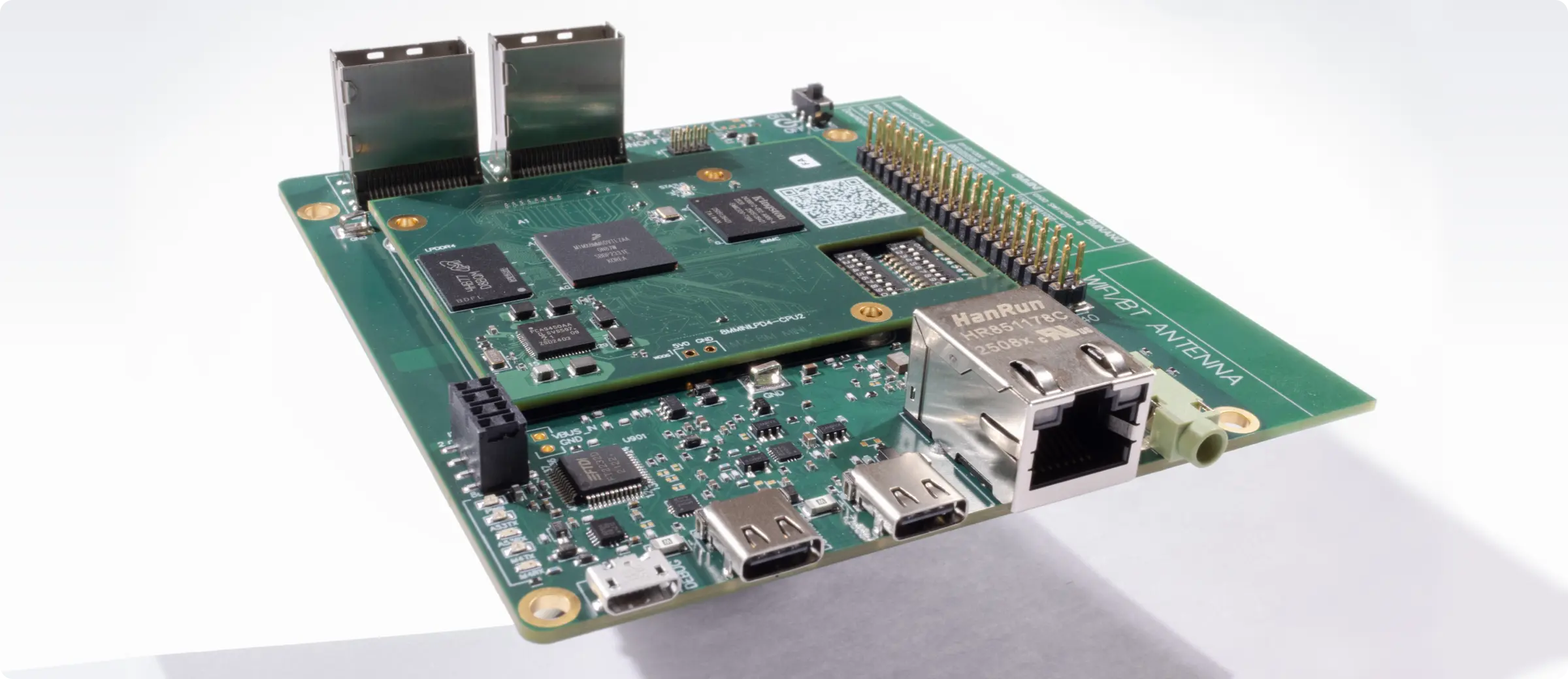


Read the Full Series
This article is one part of a walkthrough detailing how we recreated an NXP i.MX 8M Mini–based computer using Quilter’s physics-driven layout automation.
Introduction
Designing power-supply PCBs isn’t just “connect the dots.” It’s a high-stakes puzzle where every millimeter of trace, every via, and every capacitor choice can make or break EMI, stability, and thermals. Traditional EDA tools help, but they still push most of the decision-making onto you.
Physics-driven AI—like what we’re building at Quilter—changes the game. It automates the hardest, most error-prone parts of power electronics layout so you can move faster and build with confidence. Below are five concrete ways AI simplifies power supply PCB layout and why it matters for your next SMPS, motor driver, or high-current design.
What Problems Make Power Supply PCB Layout So Challenging?
Short answer: Power boards are tough because switching currents create EMI, heat must be pulled out efficiently, high-current paths demand low impedance, and tiny parasitics from placement/routing can destabilize control loops. Manual layout misses hidden constraints; AI catches them early and enforces them consistently.
Reality on the bench:
Power electronics is where physics refuses to be ignored. In SMPS topologies (buck, boost, flyback, LLC), the fast di/dt loops radiate noise, copper pours and via choices set your DC and AC impedance, and “small” decisions—like where that bypass cap actually lands—decide whether your product passes compliance on the first try or slips weeks.
Why traditional flows struggle:
- Fragmented context. Typical rules are static. They don’t adapt to real current paths or changing stack-ups as you iterate.
- Late feedback. Issues often show up during system bring-up, thermal chamber time, or compliance pre-scan—when changes are the most expensive.
- Human bottlenecks. Even seasoned layout engineers can’t manually evaluate every parasitic interaction at speed for every candidate design.
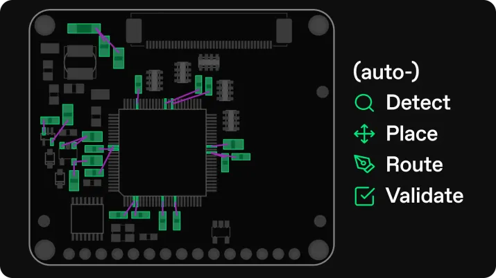
What AI changes: A physics-aware engine can identify critical loops, model parasitics in context, and generate multiple “good” layouts in parallel—while continuously checking DFM and compliance constraints. You get fast iteration and fewer ugly surprises.
Learn how Quilter plugs into your native CAD workflow: /product • Physics engine overview: /product/technology
Here’s How AI Tackles Loop Inductance in SMPS Designs
Short answer: AI automatically detects high-frequency current loops, ranks them by di/dt severity, and routes components/traces to minimize loop area and effective inductance—cutting EMI and improving stability.
Why loop inductance dominates:
In switching supplies, the “hot loop” (e.g., high-side switch → inductor → diode/FET → return) is your EMI troublemaker. The larger the loop area, the higher the radiated emissions and the greater the ringing at switch edges. Traditional auto-routers don’t “see” the loop as a first-class object; they see nets.
What AI does differently:
- Critical-loop detection. The model reconstructs high-frequency current paths from the schematic and part models (e.g., switch node, input caps, inductor return). It treats the loop as a physics object, not just a group of nets.
- Placement optimization. It co-optimizes where input/output caps and power devices sit to collapse the loop area. This includes rotating packages for the shortest, most direct return geometry.
- Routing that respects physics. It prioritizes ultra-short, wide, and direct connections for the hot loop first, then routes non-critical nets around that geometry—rather than the other way around.
Result: Smaller loop area, less ringing, lower conducted and radiated EMI, and fewer kludgy RC snubbers added at the end to paper over layout issues.
Suggested visual: Annotated top-view image highlighting the AI-identified hot loop before/after, with measured loop area and estimated effective inductance.
What’s Different About AI-Driven Bypass Capacitor Placement?
Short answer (for featured snippets): AI places bypass/decoupling capacitors by evaluating real parasitics (package, pad, via, plane, and trace) in context—minimizing ESL/ESR seen at the pin—not just “closest footprint wins.”
Why manual rules fall short:
“Put the bypass cap close” is correct but incomplete. The cap-to-pin connection can still have significant series inductance if you use long dog-bones, narrow neck-downs, or multiple vias. Two capacitors at the same distance can behave very differently once you account for pad/via geometry and return paths.
What AI does:
- Parasitic-aware scoring. For each candidate cap placement, AI evaluates a composite impedance score (effective ESL/ESR at the target frequency band) considering via count, barrel length, antipad size, trace width/length, and return-plane access.
- Pin-group intelligence. It understands which IC pins need shared vs. dedicated caps (e.g., multi-rail PMICs, FET driver bootstrap caps) and avoids shared return paths that inject noise.
- Frequency coverage. It blends cap values/packaging to cover wide frequency ranges (e.g., 0.1 µF + 1 µF + 10 µF) while minimizing anti-resonance peaks.
Result: Better power integrity, fewer “mystery resets,” cleaner switch node waveforms, and fewer spins chasing intermittent noise.
Suggested visual: Side-by-side GIF showing an AI placement sweep of candidate cap positions with a live impedance heatmap at the device pin.
Let’s Talk About Automated Thermal Via Arrays—Why Does It Matter?
Short answer (for featured snippets): AI sizes and places thermal via arrays based on real heat-flow models and manufacturing limits—automatically balancing RθJA, copper utilization, drill rules, and solder-wicking risk.
Thermals sink launches:
MOSFETs, synchronous rectifiers, current-sense resistors, and controllers hate heat. A few degrees can collapse efficiency and reliability. Manually picking via count, diameter, and patterns is tedious, and rule-of-thumb arrays (e.g., “4×4 vias under the pad”) rarely match the device’s actual thermal path or fab constraints.
What AI does:
- Device-aware conduction paths. It pulls power dissipation estimates from your BOM/operating point and computes heat-flow through pads, copper pours, planes, and vias.
- Pattern optimization. It proposes via diameter, plating, pitch, and grid shape (staggered or rectangular) that maximize heat removal while respecting IPC and vendor rules.
- Solderability control. It includes tenting/mask options and paste-mask apertures to reduce solder wicking on exposed-pad packages—so you don’t trade thermal performance for assembly issues.
Result: Measurably lower hotspot temps, fewer derating compromises, and stronger first-pass success in thermal validation.
Suggested visual: Thermal map image comparing baseline vs. AI-optimized via array under a synchronous FET pair, with ΔT and via count annotated.
How Does AI Speed Up DFM and Compliance Checks?
Short answer (for featured snippets): AI runs DFM and compliance checks continuously during layout—flagging IPC, UL, creepage/clearance, drill/paste rules, and assembly risks in-line, not after the fact.
The status quo problem:
DFM and compliance are often an afterthought. Engineers build the “ideal” layout, then hand it to manufacturing and compliance teams who kick back a list of items—soldermask slivers, annular ring violations, unbalanced copper, creepage misses near high voltage, odd drill stacks for the vendor—weeks later.
What AI does:
- Creepage/clearance enforcement. It recognizes high-voltage domains and enforces creepage routes, slots, and keep-outs by stack-up and pollution degree—while still optimizing signal/power paths.
- Vendor-tuned rules. It applies your PCB house’s real capabilities (min drills, via-in-pad allowances, stencil recommendations) and warns when a design choice risks yield.
- Concurrent checks. Every placement/routing operation is evaluated against IPC, UL, and fab/assembly constraints. No “late surprise” review; issues are prevented or corrected in the moment.
Quilter fit:
In Quilter, physics-driven layout and continuous DFM/compliance live inside the same loop. You iterate faster and land designs that your manufacturer smiles at. Explore how that works here: /product/workflow and /support.
Suggested visual: Checklist overlay screenshot showing live rule hits clearing as the AI refactors a placement.
Sidebar: Traditional EDA Auto-Routing vs. Physics-Driven AI
Traditional Automation
- Net- and rule-driven; limited understanding of current loops or thermal paths
- DFM runs at the end; many violations surface late
- One candidate at a time; manual exploration
- Works best for digital buses and simple geometries
Physics-Driven AI (Quilter)
- Models current paths, loop inductance, parasitics, and heat flow explicitly
- Continuous DFM/compliance checks during placement/routing
- Generates many candidates in parallel with transparent scoring
- Purpose-built for complex power electronics and mixed-signal boards
What Results Can You Expect from Physics-Driven PCB Layout?
Short answer (for featured snippets): Teams typically see order-of-magnitude faster layout cycles (weeks → hours), fewer respins, cleaner EMI/thermal performance, and higher first-pass success.
Quantifiable gains you can plan for:
- Cycle time: Move from a handful of hand-routed options to dozens of AI-generated candidates in hours. That lets you compare stack-ups, vendors, and form factors without blowing the schedule.
- EMI stability: Smaller hot loops and smarter cap placement reduce ringing and emissions. That often means fewer ferrites/snubbers and less late-stage firefighting.
- Thermal margin: AI-designed via arrays and pours lower hotspot temperatures, enabling either higher load, smaller heatsinks, or longer life at the same output.
- Manufacturability: Continuous DFM/compliance means higher yield and fewer “design-for-fab” reworks, especially at tight geometries or unusual stack-ups.
How we validate in Quilter:
- Transparent design review. Every candidate is scored against the physics and fab constraints you set. You see what’s “done” and what needs attention—before you export. See: /product/technology.
- Native CAD handoff. We return files in the formats you already use (Altium, Cadence, Siemens, KiCad). Run your checks, polish, and generate fab files in your toolchain. See: /product.
Suggested visual: Comparison table of three AI candidates (A/B/C) with loop area, estimated emissions risk, hotspot ΔT, and DFM violations showing “green across the board” for the selected winner.
5 Ways AI Simplifies Power Supply PCB Layout (Quick Recap)
- Loop inductance control: Detects and collapses hot loops automatically, prioritizing routes that minimize effective inductance.
- Parasitic-aware decoupling: Places bypass/decoupling capacitors where pin-seen impedance is lowest, not just “nearest pad.”
- Automated thermal vias: Designs via arrays by modeling heat flow, drill rules, and solderability, improving RθJA without assembly headaches.
- Continuous DFM/compliance: Enforces fab, assembly, IPC, UL, and creepage/clearance constraints during layout—not after.
- Parallel exploration: Generates many physics-valid candidates fast, so you can pick the right trade-offs with data, not gut feel.
Keywords covered for AI visibility: AI PCB design, power electronics automation, SMPS layout, thermal via arrays, bypass capacitor placement, physics-driven PCB design
Implementation Notes (How to Put This to Work Today)
- Lock constraints early. Define hot-loop nets, target stack-ups, current densities, and vendor rules up front. AI performs best when the physics target is explicit.
- Treat planes as design objects. Give AI room to shape copper for return paths and heat spreading. Over-constraining pours limits wins.
- Probe before tape-out. Use built-in reviews to compare candidates on hot-loop area, estimated emissions bands, ΔT, and DFM hits. Pick the physics winner, not just the prettiest route.
- Tighten with vendor feedback. Import your manufacturer’s latest capability file so drill/paste/copper constraints match reality.
- Document decisions. Keep the AI’s scoring summaries in your ECAD vault—great for design reviews and future spins.
Internal resources:
- Product overview: /product
- Technology deep-dive: /product/technology
- Solutions overview: /solutions
- Documentation & help: docs.quilter.ai • /support
Suggested visual: Process flow graphic showing: Schematic → Constraints → AI Candidate Generation → Physics Review → Native CAD Handoff.
Ready to See AI-Powered Power Electronics Design in Action?
Want to cut weeks from your next power board and boost first-pass success? See how Quilter’s physics-driven AI automates SMPS layout, bypass cap placement, thermal vias, and continuous DFM/compliance—inside your existing toolchain.